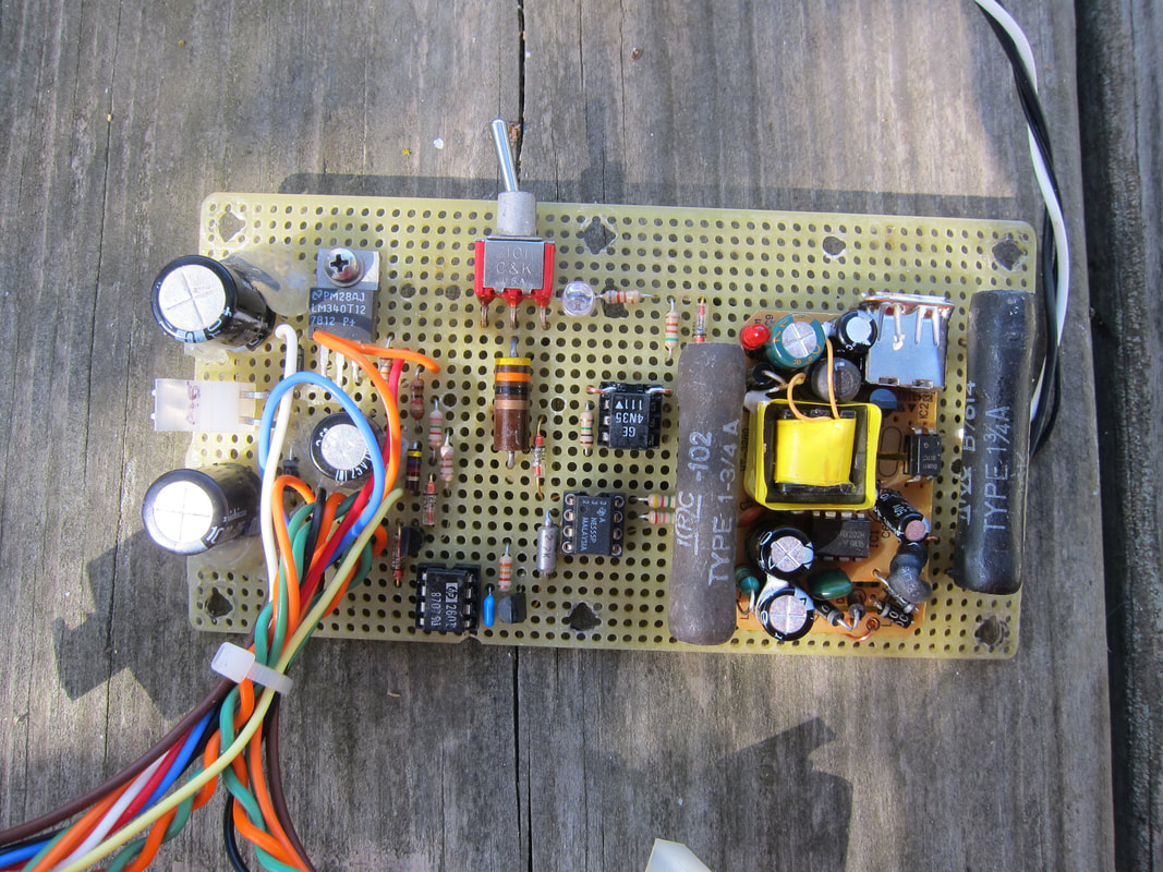
Parts List:
A1A1 (Assembly A1 is only one part of Power Control Module A1):
C1, C2; cap. 1000uF 35V, 2ea
C3; cap. 220uF 25V, 1 ea
C5; .1uF 50V, 1ea
C8; 2.2uF, 20V Tantalum, 1ea
VZ3, 5, 6, 7: zener 6.2V 1n753, 4ea
CR1, 2: diode 1KV 1A 1n4007, 2ea
R1: res 2.7M 1/4W, 1ea
R2: res 18K 1/4W, 1ea
R3: res 1K 1/4W, 1ea
R4: res 43 ohm 1W, 1ea
R5: res 4.7 M ohm, 1ea
R6: 11M ohm 1/4W, 1ea
R7, R8: res 3.3K 1/4W, 2ea
R9: res 910 ohm 1/4W, 1ea
R10: res 7.2K 1/4W, 1ea
R11: res 4.7K 1/4W, 1ea
R12: res 1 meg 1/4W, 1ea
R13: res 10K 10W, 1ea
R14: res 16K 10W, 1ea
R15: 510 ohm 1/4W, 1ea
R16: 820 ohm 1/4W, 1ea
Q1-Q2: N-FET 2N7000, 2ea
U1: optoisolator GE 4N35, 1ea
U1X: IC socket 6-pin, 1ea
U2: 12V regulator LM7812T, 1ea
U3: optoisolator HCPL 2601, 1ea
U3X, U4X: IC socket 8-pin, 2ea
U4: TIMER NE555, 1ea
LED1: LED RED 4MM, 1ea
SW1, STDT, PCB Mount, 1ea
P16: header 90 deg large M, 1ea
A1: USB Power Supply, 5V 500 MA
P20: 2 pin Molex M
J8: Molex 12 Pin F, 1ea
J18: Molex 9 Pin F, 1ea
Molex Pins F, 15ea
Molex Pins M, 2ea
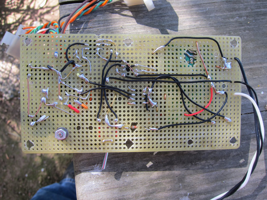
Vector Board, as needed
A1A1 (Assembly A1 is only one part of Power Control Module A1):
C1, C2; cap. 1000uF 35V, 2ea
C3; cap. 220uF 25V, 1 ea
C5; .1uF 50V, 1ea
C8; 2.2uF, 20V Tantalum, 1ea
VZ3, 5, 6, 7: zener 6.2V 1n753, 4ea
CR1, 2: diode 1KV 1A 1n4007, 2ea
R1: res 2.7M 1/4W, 1ea
R2: res 18K 1/4W, 1ea
R3: res 1K 1/4W, 1ea
R4: res 43 ohm 1W, 1ea
R5: res 4.7 M ohm, 1ea
R6: 11M ohm 1/4W, 1ea
R7, R8: res 3.3K 1/4W, 2ea
R9: res 910 ohm 1/4W, 1ea
R10: res 7.2K 1/4W, 1ea
R11: res 4.7K 1/4W, 1ea
R12: res 1 meg 1/4W, 1ea
R13: res 10K 10W, 1ea
R14: res 16K 10W, 1ea
R15: 510 ohm 1/4W, 1ea
R16: 820 ohm 1/4W, 1ea
Q1-Q2: N-FET 2N7000, 2ea
U1: optoisolator GE 4N35, 1ea
U1X: IC socket 6-pin, 1ea
U2: 12V regulator LM7812T, 1ea
U3: optoisolator HCPL 2601, 1ea
U3X, U4X: IC socket 8-pin, 2ea
U4: TIMER NE555, 1ea
LED1: LED RED 4MM, 1ea
SW1, STDT, PCB Mount, 1ea
P16: header 90 deg large M, 1ea
A1: USB Power Supply, 5V 500 MA
P20: 2 pin Molex M
J8: Molex 12 Pin F, 1ea
J18: Molex 9 Pin F, 1ea
Molex Pins F, 15ea
Molex Pins M, 2ea
Vector Board, as needed
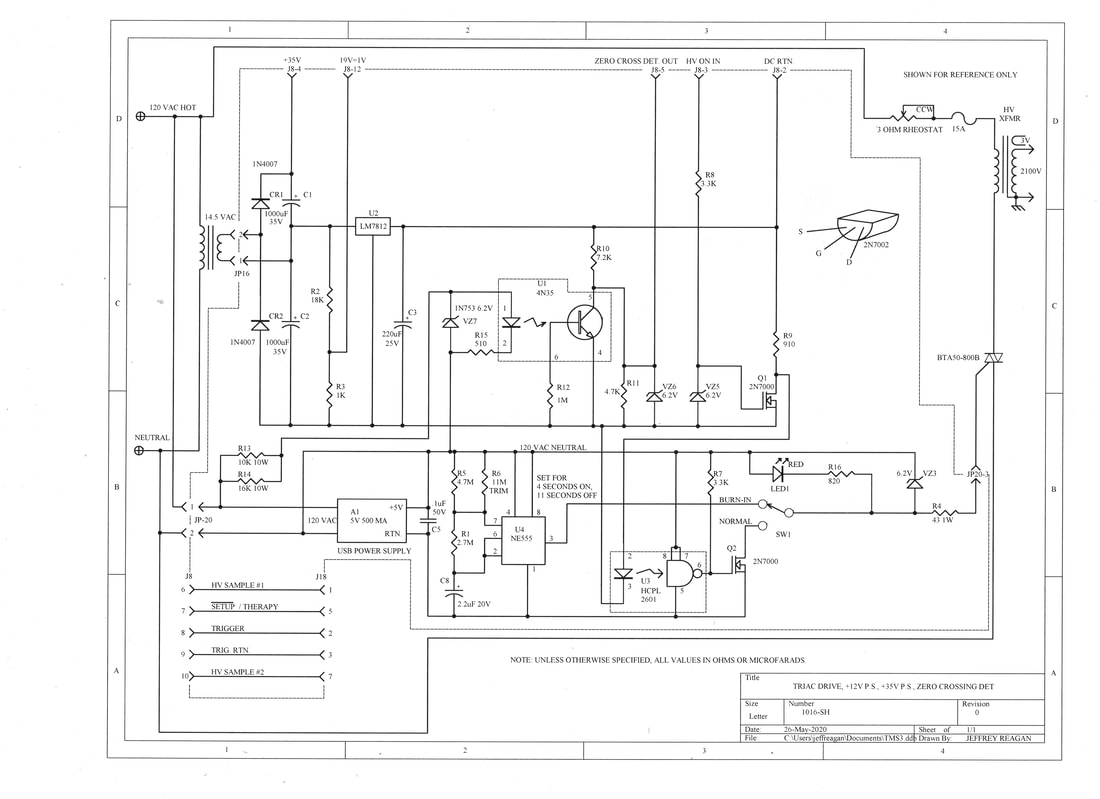
Triacs are driven here with negative polarity gate drive current (less than 100 milliamps). A HIGH VOLTAGE ON command signal enters via connector J-8 pin 3, driving FET Q3 ON. Optoisolator U3 loses drive current at pin-2. The inverting output stage of U3 switches HIGH, which drives FETs Q2 and Q1 ON respectively, in rapid succession (with Q2 energizing first, then Q1). Q2 drives external Step-Start Triac (A1A4) ON, delivering line voltage through a 10 Ohm 25 Watt resistor to the high voltage transformer primary. R1 charges C4 to energize Q1, which drives external Triac (A1A3) ON, thus bypassing the 10 Ohm resistor to deliver line voltage directly to the high voltage transformer primary. The ON STATE lasts 4 seconds. The HIGH VOLTAGE ON command vanishes: U3 output switches Low, shutting off both Q1 and Q2 promptly (also discharging C4 via CR3). Both Triacs lose gate drive almost simultaneously. OFF-TIME lasts 11 seconds. This cycle repeats, lasting 13 minutes for therapy, or indefinitely in the Burn-In Mode, which can be selected using an external computer.
A line-voltage referenced floating 5 Volt supply powers Optocoupler U3, also providing Triac Gate Drive current (which comes from Transformer T1, via bridge rectifier CR4-CR7, Capacitor C6, 5-Volt-Regulator U4, and bypass capacitors C5, C7, and C8).
Arduino power and Pulse Regulator Board power come from a Ground-Referenced voltage doubler (comprised of diodes CR1, CR2, capacitors C1, and C2, powered via connector JP16 by an off-board 14.5 Volt transformer). Raw +35 Volts is fed to the pulse regulator board via connector J8 pin 4. Semi-regulated +12 Volts ports to the Pulse Regulator Board via J8-Pin 1. (The +12 volt output drops to 11 Volts under load, but this feeds a downstream 8 Volt regulator, so poor regulation is of no consequence.) A sample of the +12 Volt regulator raw supply input is divided down to under 1 Volt (by R2 and R3), which gets fed into Arduino Analog input A1. This input isn't used by current code. DC current returns via ground referenced J8 pin 2.
Line Voltage Zero Crossing Detection is done by Optocoupler U1. Line voltage passes through parallel resistors R13 and R14 to be zener clamped at 6.2 Volts, then fed to U1 input LED via R15. Roughly square wave output results, emerging from Optocoupler output (pin 5). The signal is developed by a voltage divider (R10 and R11) fed from local +12 Volts, producing a TTL level output signal for Arduino Digital Input D8. This signal isn't used by current code. Eventually Phase Control will be used to adjust pulse output power, eliminating the need for a Rheostat.

TMS Design by Jeffrey Philip Reagan is licensed under a Creative Commons Attribution-ShareAlike 4.0 International License.
